FAN48632
FAN48632 is Pulsed-Load Synchronous Regulator manufactured by onsemi.
Pulsed-Load Synchronous Regulator with Bypass Mode for GSM PA Supply, TINYBOOST), 2.5 MHz, 2.0 A
Description The FAN48632 allows systems to take advantage of new battery chemistries that can supply significant energy when the battery voltage is lower than the required voltage for system power ICs. By bining built- in power transistors, synchronous rectification, and low supply current; this IC provides a pact solution for systems using advanced Li- Ion battery chemistries.
The FAN48632 is a boost regulator designed to provide a minimum output voltage (VOUT(MIN)) from a single- cell Li- Ion battery, even when the battery voltage is below system minimum. In boost mode, output voltage regulation is guaranteed to a maximum load current of 1.5 A continuous and 2.0 A pulsed. Quiescent current in Shutdown Mode is less than 3 m A, which maximizes battery life. The regulator transitions smoothly between Bypass and normal Boost Mode. The device can be forced into Bypass Mode to reduce quiescent current.
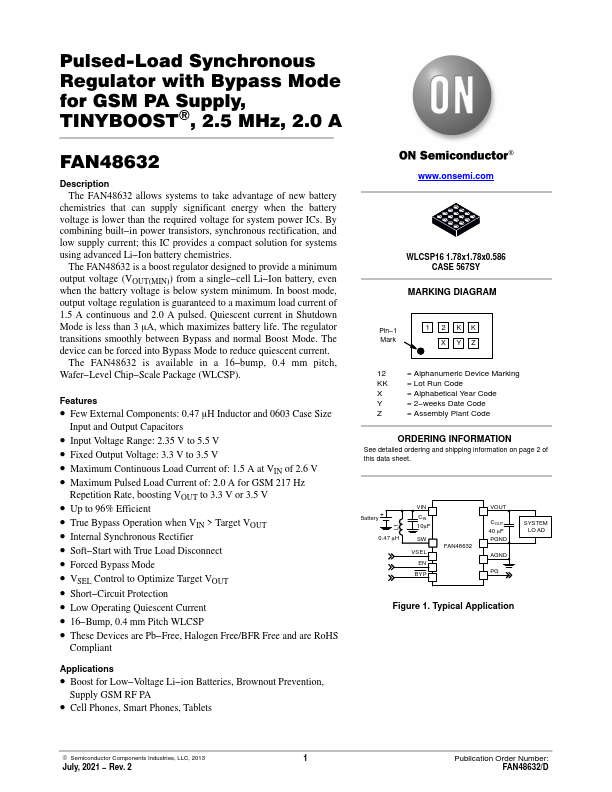
The FAN48632 is available in a 16- bump, 0.4 mm pitch, Wafer- Level Chip- Scale Package (WLCSP).
Features
- Few External ponents: 0.47 m H Inductor and 0603 Case Size
Input and Output Capacitors
- Input Voltage Range: 2.35 V to 5.5 V
- Fixed Output Voltage: 3.3 V to 3.5 V
- Maximum Continuous Load Current of: 1.5 A at VIN of 2.6 V
- Maximum Pulsed Load Current of: 2.0 A for GSM 217 Hz
Repetition Rate, boosting VOUT to 3.3 V or 3.5 V
- Up to 96% Efficient
- True Bypass Operation when VIN > Target VOUT
- Internal Synchronous Rectifier
- Soft- Start with True Load Disconnect
- Forced Bypass Mode
- VSEL Control to Optimize Target VOUT
- Short- Circuit Protection
- Low Operating Quiescent Current
- 16- Bump, 0.4 mm Pitch WLCSP
- These Devices are Pb- Free, Halogen Free/BFR Free and are Ro HS pliant
Applications
- Boost for Low- Voltage Li- ion Batteries, Brownout Prevention,
Supply GSM RF PA
- Cell Phones, Smart Phones, Tablets
.onsemi.
WLCSP16 1.78x1.78x0.586 CASE...